Introduction
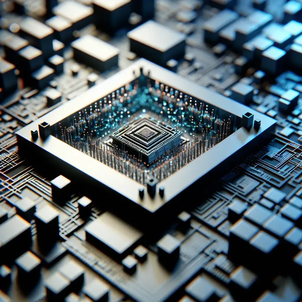
In a monumental leap for semiconductor technology, Intel has recently unveiled its groundbreaking 2nm process node, achieving a remarkable transistor density that exceeds 300 million transistors per square millimeter. This achievement not only marks a significant milestone in Intel’s relentless pursuit of smaller, more efficient chips but also sets a new benchmark in the semiconductor industry. In this article, we will explore the technical aspects of this innovation, its historical context, and what it means for the future of computing.
The Evolution of Semiconductor Technology
The journey toward smaller transistors began in the 1970s with the introduction of the microprocessor. At that time, the maximum transistor density was measured in thousands per mm². Over the decades, technological advancements such as photolithography, materials science, and chip design have allowed manufacturers to pack more transistors into smaller spaces. Intel’s introduction of the 2nm process node reflects years of research and innovation, following its 3nm and 5nm predecessors.
The Importance of Transistor Density
Transistor density is a crucial factor in determining the performance and power efficiency of chips. Higher density allows for more computations per second while consuming less power, which is vital for everything from personal computers to large-scale data centers. With Intel’s new 2nm process, the unprecedented density of over 300 million transistors per mm² will enable manufacturers to create smaller, faster, and more energy-efficient devices.
Technical Innovations Behind the 2nm Process Node
Intel’s latest innovation is built on several key technological advancements:
- New Materials: The transition from silicon to advanced materials such as germanium and graphene has paved the way for efficient electron movement and improved performance.
- FinFET Technology: The use of FinFET transistors in earlier nodes has allowed for better control of the current flow, which is crucial at smaller sizes.
- Extreme Ultraviolet Lithography (EUV): EUV technology enables the creation of intricate patterns on silicon wafers, allowing for the placement of transistors with extreme precision.
Historical Context
Intel’s journey to the 2nm process node is rooted in a history of innovation. The company has consistently pushed the boundaries of technology, starting with the introduction of the 4004 microprocessor in 1971, which contained just 2,300 transistors. Over the years, Intel’s development of technology nodes has changed the landscape of computing, establishing standards that other companies strive to meet.
Future Predictions: What Lies Ahead?
The unveiling of the 2nm process node signifies not only a leap in technology but also opens up new possibilities for the future. Experts predict that as this technology becomes mainstream, we can expect:
- Enhanced Performance: Computers and data centers will operate at unprecedented speeds, enabling applications that require massive processing power.
- Extended Battery Life: Devices powered by 2nm chips will likely see significant improvements in battery efficiency, benefiting mobile devices, laptops, and IoT devices.
- Advancements in AI and Machine Learning: The enhanced computational power will facilitate more complex algorithms and machine learning models that require significant processing capabilities.
Pros and Cons of the 2nm Technology
Pros:
- Increased performance and processing speed.
- Lower power consumption leading to energy-efficient devices.
- Greater integration of features and capabilities in smaller devices.
Cons:
- The increased complexity in manufacturing processes may lead to higher production costs.
- Potential challenges in heat dissipation as transistor density increases.
- Need for new materials and technologies that may require further research and development.
Real-World Applications
The implications of Intel’s 2nm process are far-reaching. Here are several real-world applications that stand to benefit:
- Consumer Electronics: Future smartphones and laptops will benefit significantly from improved performance and battery life, enhancing user experience.
- Data Centers: With increased processing power and efficiency, data centers can better handle the exponential growth in data traffic and cloud computing demands.
- Artificial Intelligence: More powerful chips will accelerate AI processing, enabling applications like autonomous vehicles, smart cities, and healthcare diagnostics.
Conclusion
Intel’s unveiling of the 2nm process node with a transistor density exceeding 300 million per mm² is not just a significant technological advancement; it is a testament to human ingenuity and the relentless drive for progress in the semiconductor industry. As we stand on the brink of this new era in computing, we can only imagine the possibilities and innovations that await us. This milestone will undoubtedly influence the evolution of technology, shaping our devices and the world around us for years to come.